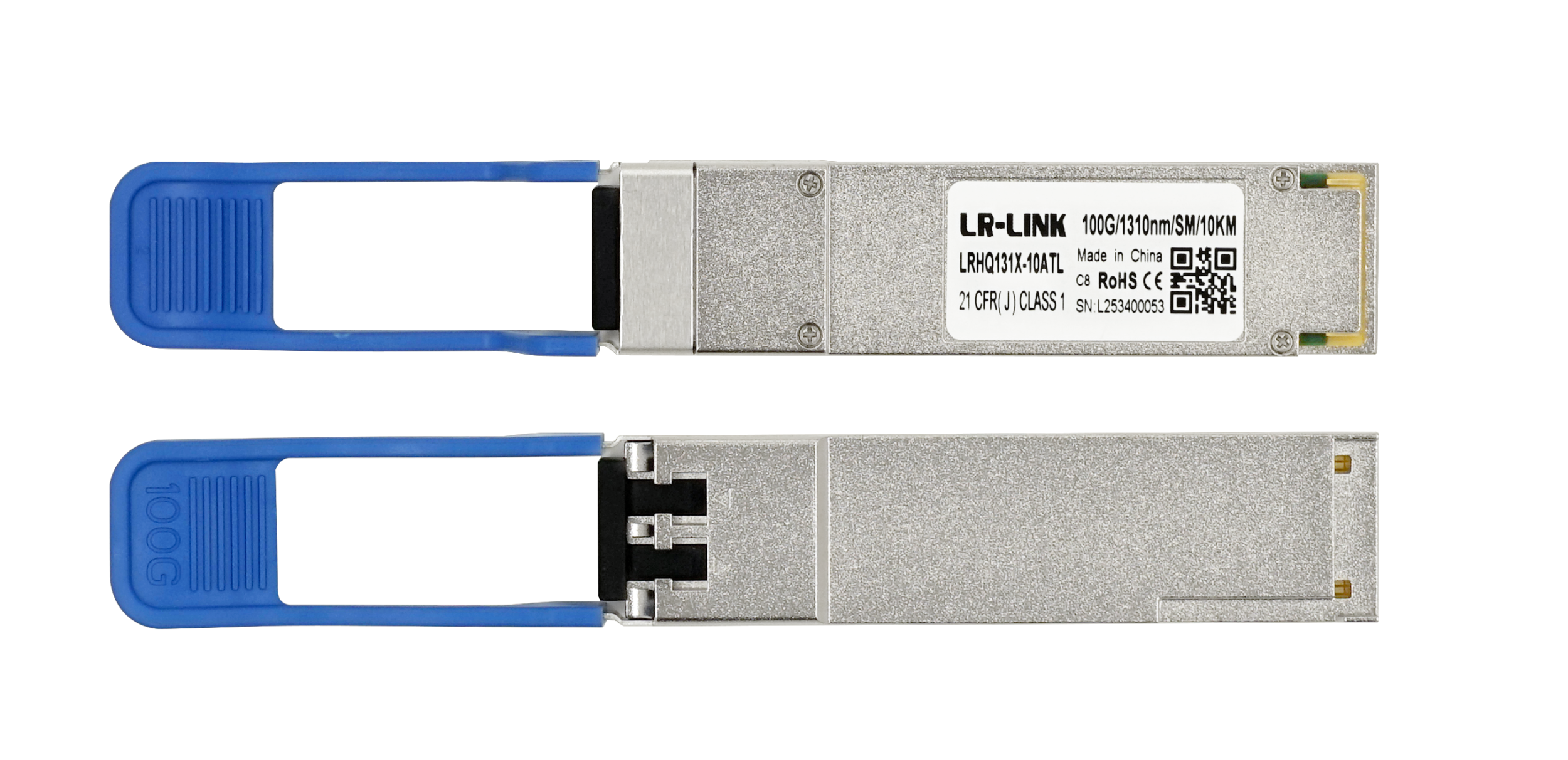
100G QSFP28 LR4 Optical Transceiver
Absolute Maximum Ratings
Parameter | Unit | Min. | Typical | Max. | Notes | |
Storage Temperature | °C | -40 | 85 | |||
Operating Relative Humidity | % | 85 | ||||
Power Supply Working Voltage | V | -0.5 | 3.63 | |||
Damage Threshold, each Lane | dBm | 5.5 |
Recommended Operating Conditions
Parameter | Unit | Min. | Typical | Max. | Notes | |
Operating Case Temperature | °C | 0 | 70 | |||
Power Supply Working Voltage | V | 3.135 | 3.135 | 3.135 | ||
Data Rate, each Lane | Gbps | 25.78125 | ||||
Power Consumption | W | 3.5 | ||||
Supply Current | A | 1.12 | ||||
Optical Characteristics
All performance is defined over the recommended operating environment unless otherwise specified.
Parameter | Unit | Min | Typical | Max | Notes | |
Wavelength Assignment | nm | 1294.53 | 1295.56 | 1296.59 | ||
nm | 1299.02 | 1300.05 | 1301.09 | |||
nm | 1303.54 | 1304.58 | 1305.63 | |||
nm | 1308.09 | 1309.14 | 1310.19 | |||
Transmitter | ||||||
Side Mode Suppression Ratio | dB | 30 | ||||
Total Average Launch Power | dBm | 10.5 | ||||
Average Launch Power, each Lane | dBm | -4.3 | 4.5 | |||
OMA, each Lane | dBm | -1.3 | 4.5 | 1 | ||
Difference in Launch Power | dB | 5 | ||||
Launch Power in OMA minus Transmitter and Dispersion Penalty (TDP), each Lane | dBm | -2.3 | ||||
TDP, each Lane | dB | 2.2 | ||||
Extinction Ratio | dB | 4 | ||||
Relative Intensity Noise | dB/Hz | -130 | ||||
Optical Return Loss Tolerance | dB | 20 | ||||
Transmitter Reflectance | dB | -12 | ||||
Eye Mask{X1, X2, X3, Y1, Y2, Y3} | {0.25, 0.4,0.45, 0.25,0.28, 0.4} |
2 | ||||
Average Launch Power OFF Transmitter, each Lane | dBm | -30 | ||||
Receiver | ||||||
Damage Threshold, each Lane | dBm | 5.5 | 3 | |||
Total Average Receive Power | dBm | 10.5 | ||||
Average Receive Power, each Lane | dBm | -10.6 | 4.5 | |||
Receive Power (OMA), each Lane | dBm | 4.5 | ||||
Receiver Sensitivity (OMA), each Lane | dBm | -8.6 | ||||
Stressed Receiver Sensitivity (OMA), each Lane | dBm | -6.8 | 4 | |||
Receiver Reflectance | dB | -26 | ||||
Difference in Receive Power between any Two Lanes (OMA) | dB | 5.5 | ||||
LOS Assert | dBm | -24 | -13.6 | |||
LOS Deassert | dBm | -11.6 | ||||
LOS Hysteresis | dB | 1.5 | ||||
Receiver Electrical 3 dB upper Cutoff Frequency, each Lane | GHz | 31 | ||||
Conditions of Stress Receiver Sensitivity Test | 5 | |||||
Vertical Eye Closure Penalty, each Lane | dB | 1.8 | ||||
Stressed Eye J2 Jitter, each Lane | UI | 0.3 | ||||
Stressed Eye J9 Jitter, each Lane | UI | 0.47 | ||||
Note:
1.Even if the TDP < 1 dB, the OMA min must exceed the minimum value specified here
2.See Figure 1 below.
3.The receiver shall be able to tolerate, without damage, continuous exposure to a modulated optical input signal having this power level on one lane. The receiver does not have to operate correctly at this input power.
4.Measured with conformance test signal at receiver input for BER = 1x10-12 .
5.Vertical eye closure penalty and stressed eye jitter are test conditions for measuring stressed receiver sensitivity. They are not characteristics of the receiver.
Electrical Specifications
Parameter | Unit | Min. | Typical | Max. | Notes |
Electrical | |||||
Differential input impedance | ohm | 90 | 100 | 110 | |
Differential Output impedance | ohm | 90 | 100 | 110 | |
Differential input voltage amplitude | mVp-p | 190 | 900 | ||
Differential output voltage amplitude | mVp-p | 300 | 850 | ||
LVTTL Output High | V | 2.0 | VCC+0.3 | ||
LVTTL Output Low | V | 0 | 0.4 | ||
LVTTL Input High | V | 2.0 | VCC+0.3 | ||
LVTTL Input Low | V | VEE-0.3 | 0.8 |
PIN Function Definitions
Pin No. | Symbol | Level / Logic | Description |
1 | GND | Module Ground | |
2 | Tx2n | CML-I | Transmitter Inverted Data Input |
3 | Tx2p | CML-I | Transmitter Non-Inverted Data Input |
4 | GND | Module Ground | |
5 | Tx4n | CML-I | Transmitter Inverted Data Input |
6 | Tx4p | CML-I | Transmitter Non-Inverted Data Input |
7 | GND | Module Ground | |
8 | ModSelL | LVTTL-I | Module Select |
9 | ResetL | LVTTL-I | Module Reset |
10 | VccRx | +3.3V Power Supply for Receiver | |
11 | SCL | LVTTL-I | 2-Wire Serial Interface Clock |
12 | SDA | LVTTL-I/O | 2-Wire Serial Interface Data Line |
13 | GND | Module Ground | |
14 | Rx3p | CML-O | Receiver Non-Inverted Data Output |
15 | Rx3n | CML-O | Receiver Inverted Data Output |
16 | GND | Module Ground | |
17 | Rx1p | CML-O | Receiver Non-Inverted Data Output |
18 | Rx1n | CML-O | Receiver Inverted Data Output |
19 | GND | Module Ground | |
20 | GND | Module Ground | |
21 | Rx2n | CML-O | Receiver Inverted Data Output |
22 | Rx2p | CML-O | Receiver Non-Inverted Data Output |
23 | GND | Module Ground | |
24 | Rx4n | CML-O | Receiver Inverted Data Output |
25 | Rx4p | CML-O | Receiver Non-Inverted Data Output |
26 | GND | Module Ground | |
27 | ModPrsL | LVTTL-O | Module Present |
28 | IntL | LVTTL-O | Interrupt |
29 | VccTx | +3.3V Power Supply for Transmitter | |
30 | Vcc1 | +3.3V Power Supply | |
31 | LPMode | LVTTL-I | Low Power Mode |
32 | GND | Module Ground | |
33 | Tx3p | CML-I | Transmitter Non-Inverted Data Input |
34 | Tx3n | CML-I | Transmitter Inverted Data Input |
35 | GND | Module Ground | |
36 | Tx1p | CML-I | Transmitter Non-Inverted Data Input |
37 | Tx1n | CML-I | Transmitter Inverted Data Input |
38 | GND |
| Module Ground |

